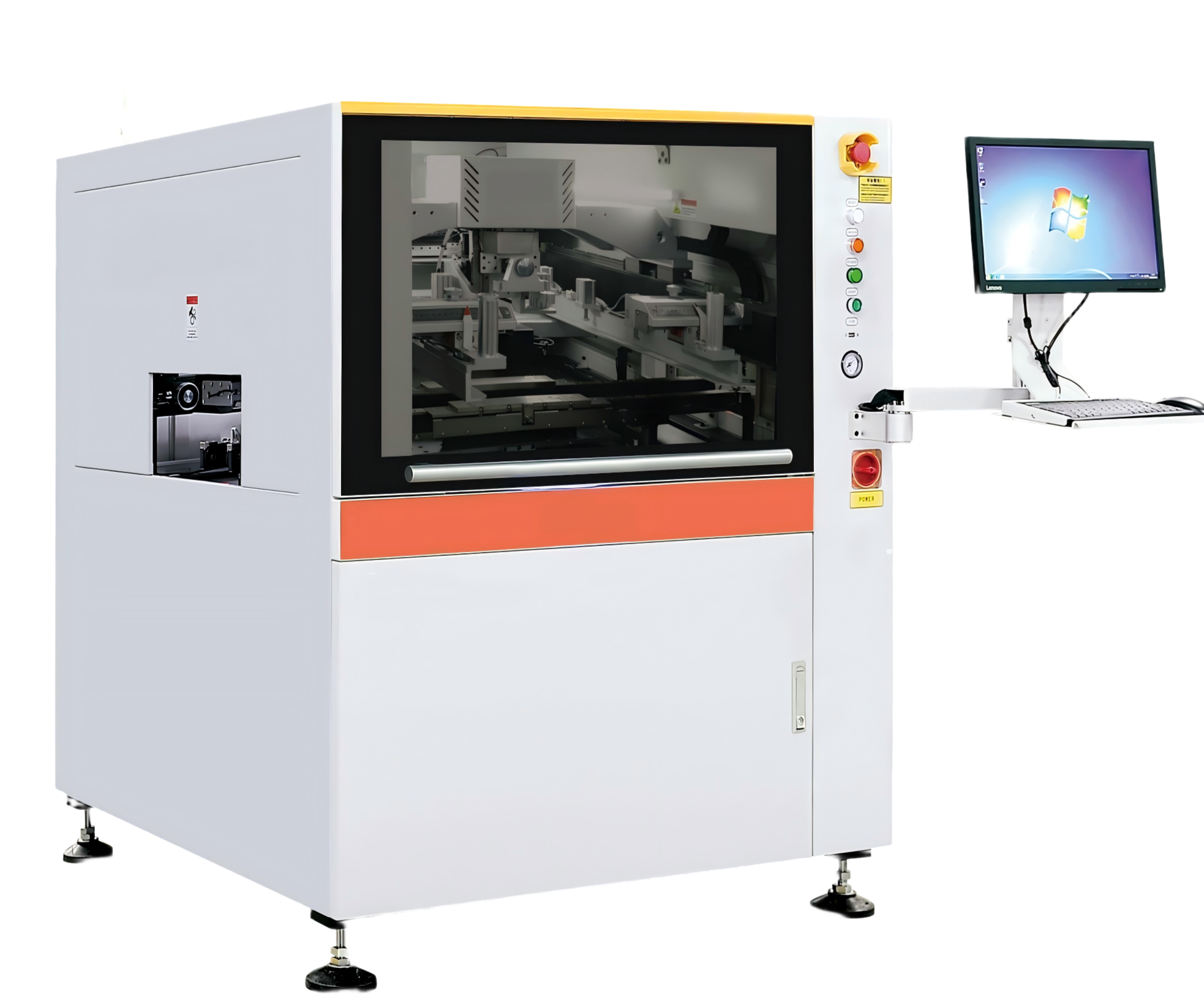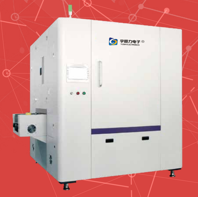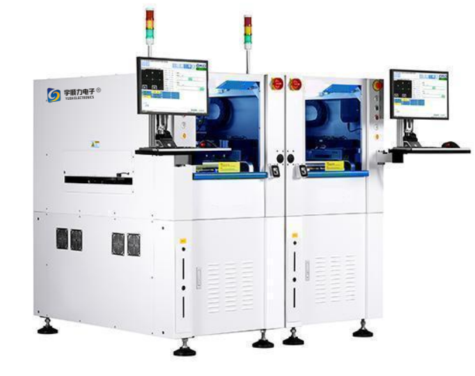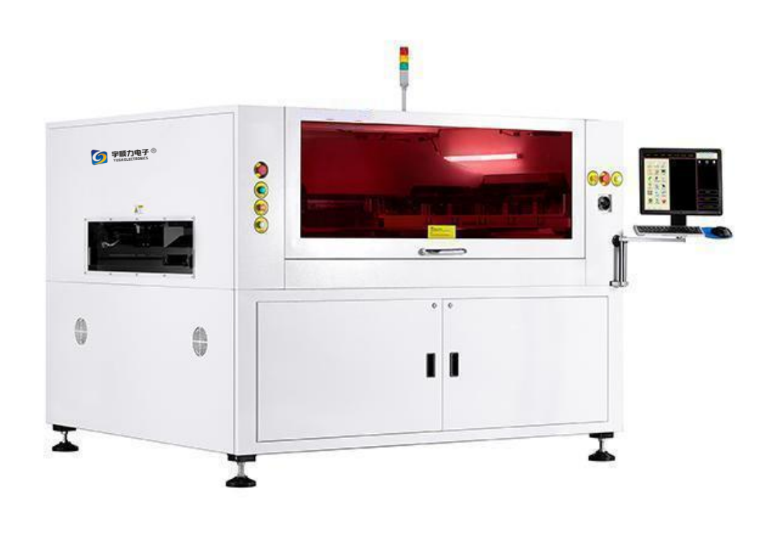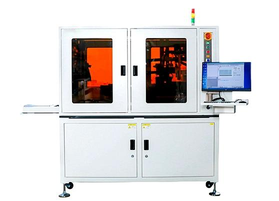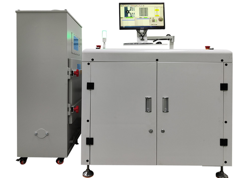
| Max PCB Size: | 600*460mm | Max Component Height: | 11mm |
|---|---|---|---|
| Laser Source: | UV, CO2 | Cutting Precision: | ±20 μm |
| Name: | PCB Laser Depaneling | Weight: | 500Kg |
Industrial PCB Laser Depaneling with Different Laser Source 10/12/15/18W
PCB depaneling (singulation) laser machines and systems have been gaining popularity over recent years. Mechanical depanaling/singulation is done with routing, die cutting, and dicing saw methods. However, as the boards get smaller, thinner, flexible, and more sophisticated, those methods produce even more exaggerated mechanical stress to the parts. Large boards with heavy substrates absorb these stresses better, while these methods used on ever-shrinking and complex boards can result in breakage. This brings lower throughput, along with the added costs of tooling and waste removal associated with mechanical methods.
Increasingly, flexible circuits are found in the PCB industry, and they also present challenges to the old methods. Delicate systems reside on these boards and non-laser methods struggle to cut them without damaging the sensitive circuitry. A non-contact depaneling method is required and lasers provide a highly precise way of singulation without any risk of harming them, regardless of substrate.
Challenges of Depaneling using Routing/Die Cutting/Dicing Saws
Damages and fractures to substrates and circuits due to mechanical stress
Damages to PCB due to accumulated debris
Constant need for new bits, custom dies, and blades
Lack of versatility – each new application requires ordering of custom tools, blades, and dies
Not good for high precision, multi-dimensional or complicated cuts
Not useful PCB depaneling/singulation smaller boards
Lasers, on the other hand, are gaining control of the PCB depaneling/singulation market due to higher precision, lower stress on the parts, and higher throughput. Laser depaneling can be applied to a variety of applications with a simple change in settings. There is no bit or blade sharpening, lead time reordering dies and parts, or cracked/broken edges due to torque on the substrate. Application of lasers in PCB depaneling is dynamic and a non-contact process.
Advantages of Laser PCB depaneling/singulation
No mechanical stress on substrates or circuits
No tooling cost or consumables.
Versatility – ability to change applications by simply changing settings
Fiducial Recognition – more precise and clean cut
Optical Recognition before PCB depaneling/singulation process begins. CMS Laser is one of the few companies to provide this feature.
Ability to depanel virtually any substrate. (Rogers, FR4, ChemA, Teflon, ceramics, aluminum, brass, copper, etc)
Extraordinary cut quality holding tolerances as small as < 50 microns.
No design limitation – ability to cut virtually and size PCB board including complex contours and multidimensional boards
Specification:
|
Parameter |
|
|
|
Technical parameters |
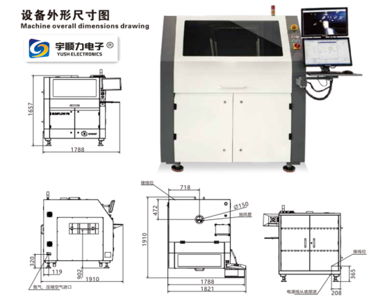
Main body of laser |
1480mm*1360mm*1412 mm |
|
Weight of the |
1500Kg |
|
|
Power |
AC220 V |
|
|
Laser |
355 nm |
|
|
Laser |
Optowave 10W(US) |
|
|
Material |
≤1.2 mm |
|
|
Precisio |
±20 μm |
|
|
Platfor |
±2 μm |
|
|
Platform |
±2 μm |
|
|
Working area |
600*450 mm |
|
|
Maximum |
3 KW |
|
|
Vibrating |
CTI(US) |
|
|
Power |
AC220 V |
|
|
Diameter |
20±5 μm |
|
|
Ambient |
20±2 ℃ |
|
|
Ambient |
<60 % |
|
|
The Machine |
Marble |
|


| Max PCB Size: | 600*460mm | Max Component Height: | 11mm |
|---|---|---|---|
| Laser Source: | UV, CO2 | Cutting Precision: | ±20 μm |
| Name: | PCB Laser Depaneling | Weight: | 500Kg |
Industrial PCB Laser Depaneling with Different Laser Source 10/12/15/18W
PCB depaneling (singulation) laser machines and systems have been gaining popularity over recent years. Mechanical depanaling/singulation is done with routing, die cutting, and dicing saw methods. However, as the boards get smaller, thinner, flexible, and more sophisticated, those methods produce even more exaggerated mechanical stress to the parts. Large boards with heavy substrates absorb these stresses better, while these methods used on ever-shrinking and complex boards can result in breakage. This brings lower throughput, along with the added costs of tooling and waste removal associated with mechanical methods.
Increasingly, flexible circuits are found in the PCB industry, and they also present challenges to the old methods. Delicate systems reside on these boards and non-laser methods struggle to cut them without damaging the sensitive circuitry. A non-contact depaneling method is required and lasers provide a highly precise way of singulation without any risk of harming them, regardless of substrate.
Challenges of Depaneling using Routing/Die Cutting/Dicing Saws
Damages and fractures to substrates and circuits due to mechanical stress
Damages to PCB due to accumulated debris
Constant need for new bits, custom dies, and blades
Lack of versatility – each new application requires ordering of custom tools, blades, and dies
Not good for high precision, multi-dimensional or complicated cuts
Not useful PCB depaneling/singulation smaller boards
Lasers, on the other hand, are gaining control of the PCB depaneling/singulation market due to higher precision, lower stress on the parts, and higher throughput. Laser depaneling can be applied to a variety of applications with a simple change in settings. There is no bit or blade sharpening, lead time reordering dies and parts, or cracked/broken edges due to torque on the substrate. Application of lasers in PCB depaneling is dynamic and a non-contact process.
Advantages of Laser PCB depaneling/singulation
No mechanical stress on substrates or circuits
No tooling cost or consumables.
Versatility – ability to change applications by simply changing settings
Fiducial Recognition – more precise and clean cut
Optical Recognition before PCB depaneling/singulation process begins. CMS Laser is one of the few companies to provide this feature.
Ability to depanel virtually any substrate. (Rogers, FR4, ChemA, Teflon, ceramics, aluminum, brass, copper, etc)
Extraordinary cut quality holding tolerances as small as < 50 microns.
No design limitation – ability to cut virtually and size PCB board including complex contours and multidimensional boards
Specification:
|
Parameter |
|
|
|
Technical parameters |
Main body of laser |
1480mm*1360mm*1412 mm |
|
Weight of the |
1500Kg |
|
|
Power |
AC220 V |
|
|
Laser |
355 nm |
|
|
Laser |
Optowave 10W(US) |
|
|
Material |
≤1.2 mm |
|
|
Precisio |
±20 μm |
|
|
Platfor |
±2 μm |
|
|
Platform |
±2 μm |
|
|
Working area |
600*450 mm |
|
|
Maximum |
3 KW |
|
|
Vibrating |
CTI(US) |
|
|
Power |
AC220 V |
|
|
Diameter |
20±5 μm |
|
|
Ambient |
20±2 ℃ |
|
|
Ambient |
<60 % |
|
|
The Machine |
Marble |
|
Website:https://www.pcbcuttingmachine.com
Contacts:Eva Liu +8613450659407 +8613416743702
Tel:+86-512-62751429
Skype:evaliuhuan
Email:caojun@hk-yush.com sales@yushunli.com evaliu@hk-yush.com
Address: Building H, GuoRui Pioneering Park,
No. 1068 Jinyang East Road, Lujia Town, Kunshan,Suzhou.
Postcode:215331
Dongguan Factory Address: 5th Floor, No.10,
Shanquan Road, Yongtou Village, Chang’an Town,
Dongguan City, Guangdong province, China.
Postcode:523843